In general, electron microscopes are considered to be extremely versatile instruments that provide a plethora of information on test samples. One important type of electron microscope is the scanning electron microscope (SEM).

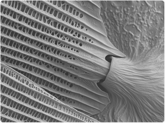
Butterfly wing under scanning electron microscopy. Image Credit: ClaudiaSEM/Shutterstock.com
Introduction
Within an SEM, a focused electron beam is emitted across the rectangular area of the test sample. In addition to the electron beam, which is the source of electrons within an SEM, some of the other primary components of an SEM include a column through which the electrons can travel, an electron detector, a sample chamber, as well as a computer and display screen that provides images to the user of the sample being analyzed.
The components of an SEM
The emitted electrons, which are produced at the top of the column, pass through the column which contains a combination of electromagnetic lenses and apertures, all of which is under vacuum. The vacuum is a crucial component of the SEM column, as it prevents any atoms and/or molecules within the column from interacting with the electron beam. By eliminating any unwanted molecular/atomic interactions, the vacuum ensures good quality imaging.
Taken together, the lenses and apertures allow for the creation of a focused electron beam that is directed towards the surface of a sample. In addition to creating a more defined electron beam, the electromagnetic lenses also control the path of the electrons, whereas the apertures assist in controlling the size of the electron beam.
Electron sources in SEMs
Within an SEM, an electron source, rather than a light beam, is located at the type of microscope. Although all electron sources are responsible for emitting a beam of highly concentrated electrons, three different electron sources can be employed in an SEM, which include thermionic filament, field emission gun (FEG), and Cerium hexaboride cathode (CeB6).
Thermionic filament
When used as an electron source for SEM, a thermionic filament, which is simply a Tungsten filament, is heated within the microscope to initiate the emission of electrons. The average lifetime of a Tungsten filament is 100 hours, as the continuous heating of this filament will cause it to gradually evaporate over time.
As the filament evaporates, it will eventually break, which can contaminate the upper part of the electron column where the filament is typically located.
FEG
A FEG is often the electron source of choice for SEMs, as it is capable of generating a strong electrical field that prevents the electrons within the beam from interacting with atoms. As a result, an SEM with a FEG electron source will typically generate high-resolution images. It should be noted, however, that a FEG electron source requires a unique vacuum design that can increase the overall cost of the microscope.
CeB6
As compared to the thermionic filament, it is estimated that the CeB6 electron source has a brightness of up to ten times greater. As the brightness increases, the signal-to-noise ratio reduces, thus providing a better resolution to the final SEM image.
In addition to improved brightness capabilities, the CeB6 electron source also has a service life of over 1,500 hours, which is fifteen times greater than that which is associated with the thermionic filament.
BSEs and SEs
As the electron beam passes through the specimen, the energy that is lost can be converted into several different types of energy, which include heat, light, secondary electrons (SEs), and backscattered electrons (BSEs). An SEM provides information on the sample through its ability to detect both SEs and BSEs.
BSEs
BSEs, which originate from deeper parts of the test sample, are reflected after elastic collisions arise between the electron beam and the atoms present within the sample. As the electrons within the beam collide with the atoms of the sample, a change in the electrons’ trajectory occurs.
The larger the atoms are within the sample, the stronger the scattering pattern, as well as the signal, will be. BSEs are typically detected by a BSE detector that is placed directly above the sample.
SEs
SEs, which typically originate from the surface or near-surface regions of the specimen, arise as a result of inelastic interactions that occur between the beam and the sample. As a result, SEs are often used to inspect the topography of a sample’s surface. As compared to the elastic interactions that result in the production of BSEs, SEs are instead the product of inelastic interactions that arise between the primary electron beam and the sample.
SEs also have a significantly lower energy level as compared to BSEs. The location of the SE detector, which is typically placed at an angle and adjacent to the electron chamber, allows for enhanced efficiency of detecting SEs, which subsequently contributes to the production of a highly detailed image of the sample’s surface.
Applications of SEM
SEMs can be used in a wide variety of industrial, commercial, and research applications, some of which include:
- Materials science
- Gas sensors
- Semiconductor quality control tools
- Microchip production
- Criminal and forensic investigations
- Biological sciences
- Geological sampling
- Diagnostics
- Digital artworks
Further Reading